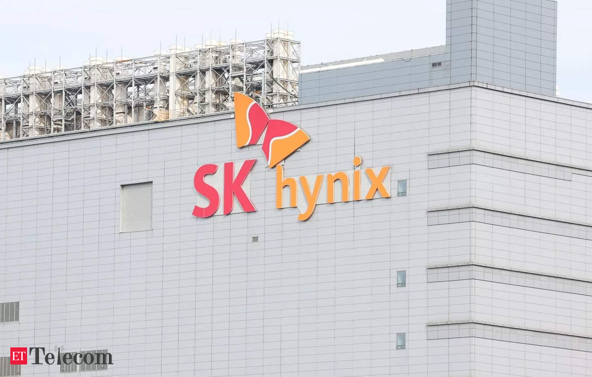
South Korean chip manufacturer SK Hynix is contemplating a significant investment opportunity in the United States, with Indiana as its potential location. The company, renowned for its innovative semiconductor solutions, has yet to finalize its decision on this venture, as stated in an official release to Reuters.
In a move to enhance its global presence and production capabilities, SK Hynix is considering establishing a cutting-edge packaging plant in Indiana. This facility will specialize in stacking standard dynamic random access memory (DRAM) chips to create high-bandwidth memory (HBM) chips.
The key objective of this venture is to streamline the production process by integrating these HBM chips directly with Nvidia’s graphic processing units (GPUs). Currently, SK Hynix manufactures its HBM chips in South Korea and then ships them to Taiwan, where they undergo integration into Nvidia’s GPUs in conjunction with other processors produced by Taiwan Semiconductor Manufacturing (TSMC).
This potential collaboration between SK Hynix and Nvidia signifies a pivotal moment in the semiconductor industry. By integrating HBM chips at a local U.S. facility, SK Hynix aims to optimize supply chain efficiency and meet the increasing demand for high-performance memory solutions. Nvidia, a leading GPU market player, can benefit from this partnership by accessing a more streamlined and efficient supply chain.
Market expansion and growth prospects
The choice of Indiana as the potential location for SK Hynix’s packaging plant aligns with the company’s vision of expanding its presence in the United States. This move not only boosts local employment opportunities but also caters to the growing demand for advanced semiconductor technologies in the region.
It is important to note that SK Hynix has not yet made a final decision on this investment, indicating that the company is still evaluating various factors, including economic incentives, logistical advantages, and regulatory considerations.
The current practice of manufacturing HBM chips in South Korea and shipping them to Taiwan for integration into Nvidia’s GPUs involves considerable time and shipping costs. By establishing a packaging plant in Indiana, SK Hynix aims to eliminate these logistical complexities and ensure a more seamless integration process.
This strategic move could significantly reduce lead times, lower transportation expenses, and enhance the overall efficiency of the supply chain. Such improvements are essential in meeting the ever-increasing demand for advanced memory solutions in the rapidly evolving tech industry.
Economic impact on Indiana
If SK Hynix proceeds with its investment in Indiana, the state is poised to reap substantial economic benefits. The creation of a state-of-the-art packaging plant will not only lead to job opportunities for residents but also contribute to the growth of Indiana’s technology sector.
Furthermore, this venture could enhance the state’s reputation as a high-tech manufacturing and innovation hub, attracting additional investment and fostering economic growth in the region.
In conclusion, SK Hynix’s exploration of a cutting-edge chip facility in Indiana marks a significant development in the semiconductor industry. The potential partnership with Nvidia and establishing a local packaging plant could streamline production, reduce shipping costs, and boost the efficiency of the supply chain. While the company has not made a final decision, the prospect of this investment holds promise for the tech industry in the United States, particularly in Indiana.
As SK Hynix continues to weigh its options, the implications of this potential venture extend beyond the company itself. The economic impact on Indiana and the broader tech sector underscores the importance of this decision, with the potential to reshape the semiconductor landscape in the United States.


